|
University of Illinois Scientists Show Us Little Known Approaches to Make More Effective Photovoltaic Panels
Article Written and Submitted by Shannon Combs
U. of Illinois
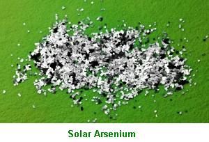
If you may decrease substantially the price of gallium arsenide and some other compound semiconductors, then you might increase their own range of applications. Typically, gallium arsenide is transferred in a individual thin layer on a little wafer. Either the needed unit is created right on the wafer, or the semiconductor-coated wafer is cut up into chips of the ideal dimension. The Illinois team decided to put in several layers of the material on a one wafer, producing a layered, “pancake” stack of gallium arsenide thin films. If you grow ten layers in one growth, you only have to fill the wafer one time. If you do this in 10 growths, loading and unloading with temp ramp-up as well as ramp-down get a lot of time. If you consider exactly what is required for each growth – the machine, the planning, the period, the people – the overhead saving this approach provides is a substantial price decrease.
Next the researchers independently peel off the levels and transport them. To achieve this, the stacks alternate levels of aluminum arsenide with the gallium arsenide. Bathing the stacks in a solution of acid and an oxidizing agent dissolves the layers of aluminum arsenide, freeing the individual thin sheets of gallium arsenide. A soft stamp-like device selects up the levels, just one at a time from the top down, for transfer to another substrate – glass, plastic or silicon, depending on the application. Next the wafer may be used again for an additional growth. By doing this it's possible to make much more material more rapidly and more price efficiently. This process could make mass amounts of material, as compared to merely the thin single-layer method in which it is generally grown. Freeing the material from the wafer additionally opens the possibility of flexible, thin-film electronics produced with gallium arsenide or some other high-speed semiconductors. To make units which may conform but still keep higher efficiency, that is considerable. In a document shared on-line May twenty in the magazine Nature, the group details its procedures and shows three kinds of products making use of gallium arsenide chips made in multilayer stacks: light units, high-speed transistors and solar cells. The authors also offer a comprehensive cost evaluation. Another advantage of the multilayer method is the release from area constraints, particularly important for photo voltaic cells. As the levels are removed from the stack, they can be laid out side-by-side on an additional substrate in order to create a much larger surface area, whereas the typical single-layer procedure confines area to the size of the wafer. For solar panels, you need big area coverage to get as much sunshine as achievable. In an extreme situation we could develop enough layers to have 10 times the area of the traditional. Next, the group plans to explore more prospective product applications and other semiconductor materials that could adapt to multilayer growth.
Shannon Combs writes for the residential solar power manufacturers web log, her personal hobby weblog centered on tips to help home owners to save energy with solar power.
|
| |||


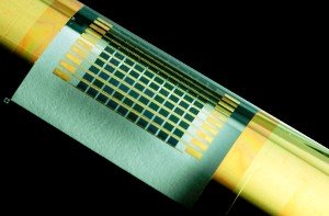 Professors J. Rogers and X. Li discovered lower-cost methods to create thin films of gallium arsenide which also allowed usefulness in the types of units they might be included into.
 About the Writer
